
Supply Features
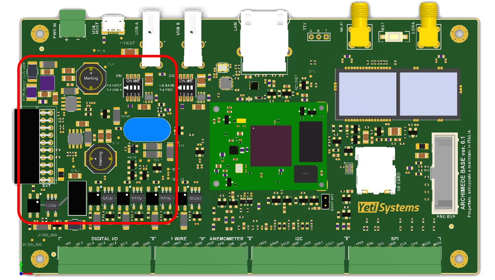
Archimedes has several power supplies in order to power all the peripherals on the board, this page explains its specifications and how to diagnose it.
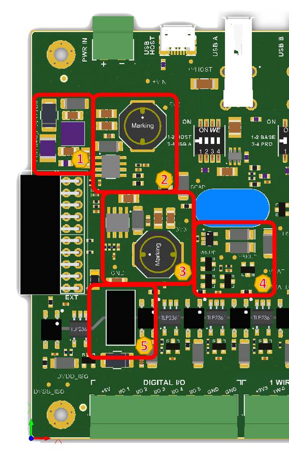
Power Supply and Power Module are GPIO manageable
| Mark | Description |
|---|---|
| 1 | Input filtering and reverse power protection |
| 2 | 5V0 Switching Power Supply |
| 3 | 3V3 Switching Power Supply |
| 4 | 3V0 LDO and Supercap Management |
| 5 | Insulated Integrated Power Module |
General Description and Input Protection:
Archimede has got several on-board power supplies that serve all the peripherals, those are protected to guarantee service and at the same time protect the equipment.
Power input is PTC fused from faulty cases and a fast recovery diode prevent wrong polarity supply.
Common mode choke with TVSs guarantee work in heavy electromagnetic perturbations cases, Furthermore strategic placed ferrite beads allow this carrier to elevate the Power Supply Rejection Rejection Ratio (PSSR) in order to have stable supply voltage with low electrical noise.
All our switching power controllers are supplied by a circuit that allows the inrush input current reduction (soft-start), in order to provide harvesting power capability as such us small photovoltaic solution in addition to reduce the battery voltage drop in extreme low climatic powered solution than can cause system fail in non-well engineered product.
Large use of MLCC and tantalum capacitors instead electrolityc type, allow this board to increase expected life time, High Quality connectors and Industrial range Integrated circuits consent this carrier to operate in the hardest climatic condition.
5V0 Power Supply:
Onboard a medium frequency switching buck type converter allow to reduce the input voltage to 5V with low loss and high performance; first class IC and discretes, allow this circuit to operate in optimal condition and provide electrical noiseless supply voltage in order to guarantee continous 2 Amperè current delivery requested by the USB standard devices as well as other peripherals.
This controller can be GPIO pin disabled in every moment for energy saving, normally during the carrier bootstrap this pin il pulled down by a resistor network that disable the module.
Two microprocessor are enabled to manage this pin trough a OR gate, one is the RoadRunner module and it’s used to manage the module in ordinary activity, one is connected instead on the L01 module, and allow to charge the supercapacitor in deep sleep mode — see dedicated page —
3V3 Power Supply:
This power supply feed all the I/O circuitry and SOM processor unit.
Onboard a fixed frequency switching buck type converter allow to reduce the input voltage to 3V3 with ultra-low ripple.
High grade ceramic capacitor use allow this circuit to high rank voltage with low remaning modulation, it means high accuracy analogic acquisition and longer discrete life considering that noisily voltage means MTBF reducing.
This controller can be disabled since this board is suspend to RAM capable.
this is possible through a supercapacitor powered circuit that keep vital power supply alive when the main power module is turned off.
— link to dedicated page—
LDO and Supercap Management:
A supercapacitor provides energy reserve when the deep-sleep modality is requested, this enable the Real Time Clock (RTC) and other stuff to work.
The supercap is 5 volt powered through a current limiting circuit, and provides two separated power outputs through a 3V0 low dropout regulator (LDO) those 2 lines independently supply RoadRunner and L01 backup circuitry when the 3V3 power module is down.
Insulated Power Supply:
An integrated module provides 5V insulated power out required for digital stuff.
It provide 1 kV RMS insulation, some precautions have become necessary to improve pcb insulation quality, as circuit board cutout to increase the opto copuler features.
Test Point and Power Supply features
Technical Information:
| TestPoint Description | Test Point ID | Nominal Value | Tollerance admitted | Temperature Drift admitted | Ripple RMS Admitted | Voltage Surge admitted |
|---|---|---|---|---|---|---|
| Input Voltage | VIN | 7 to 28 VDC | unregulated | unregulated | 1 V | 0,5 V/s² |
| 3V3 Switching Output | 3V3 | 3,35 VDC | 1% | 0.2 % | 20 mV | 0.02 V/s² |
| 5V0 Switching Output | 5V0 | 5,08 VDC | 1 % | 0.2 % | 50 mV | 0.02 V/s² |
| Supercapacitor Voltage | SCAP | 5,00 VDC | 2 % | 0.2 % | 5 mV | 0.02 V/s² |
| Supercapacitor LDO Output | 3V0 | 3,00 VDC | 2 % | 0.2 % | 5 mV | 0.02 V/s² |
| Clock Battery Voltage | VBAT | 2,70 VDC | 2 % | 0.2 % | 5 mV | 0.02 V/s² |
| Transceiver Backup Voltage | L01 | 2,70 VDC | 2 % | 0.2 % | 20 mV | 0.02 V/s² |
| A/D Voltage Reference | ADVREF | 3,30 VDC | 0.5 % | 0.2 % | 5 mV | 0.01 V/s² |
| Positive Digital Insulated Voltage | DVDD_ISO | 5,00 VDC | 5 % | 1 % | 200 mV | 0.5 V/s² |
| NegativeDigital Insulated Voltage | DVSS_ISO | 0,00 VDC | 5 % | 1 % | 20 mV | 0.5 V/s² |
Contact US
For more info or suggestions to improve the documentation